As their paper published in Journal of Material Chemistry C, FEI Guangtao’s team of Institute of Solid State Physics, Hefei Institutes of Physical Science designed a self-assembly method with special modification, and it is the first to successfully prepare ordered V2O5 nanowire arrays without any surfactant.
For photodetectors, the responsivity and response time are the important critical parameters. According to previous reports, one-dimensional (1D) semiconductor nanomaterials have been widely investigated because of their large specific surface.
However, the effective illumination area of a single nanowire is so small that causes a photocurrent of nA or pA order of magnitude, which produces barriers in its practical application to optoelectronic devices.
To remove these barriers, scientists focus on large scale structures, especially the ordered nanowire arrays one.
On the one hand, aligned nanowire arrays retain the performance merits of single nanowires and may even have an integration effect. On the other hand, these nanowire arrays have more photon-generated carrier transmission channels, which drastically improves their photocurrent values. Moreover, the arrangement of the nanowire array structure could suppress the reflection of the light, so as to improve the light trapping ability of device.
As one of the most important semiconductor nanomaterials, V2O5 with a wide bandgap of 2.3 eV and a large optical adsorption in the visible-light region. So it was considered as one of the most promising photoelectric materials.
However, it still remains as a challenge to exlpore the ordered V2O5 nanowire array structures and their corresponding optoelectronic properties.
In this work, the team designed a self-assembly method with special modification, and it is the first to successfully prepare ordered V2O5 nanowire arrays without any surfactant either in the preparation process of nanowires or in their subsequent self-assembly process.
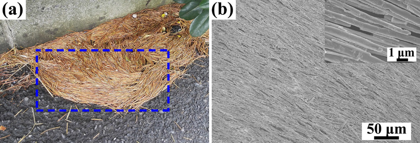
The mechanism of the nanowires self-assembling into ordered arrays are derived to the natural phenomena. Ordered pine needles that were flushed in running water, even pine needles have poor dispersion in water (Figure 1a).
The nanowires are arranged parallel in the same direction on the substrate and formed a uniform and compact array film (Figure 1b). Additionally, single layer and multiple layer ordered nanowire arrays could be achieved by controlling the precursor concentration and the assembly time,
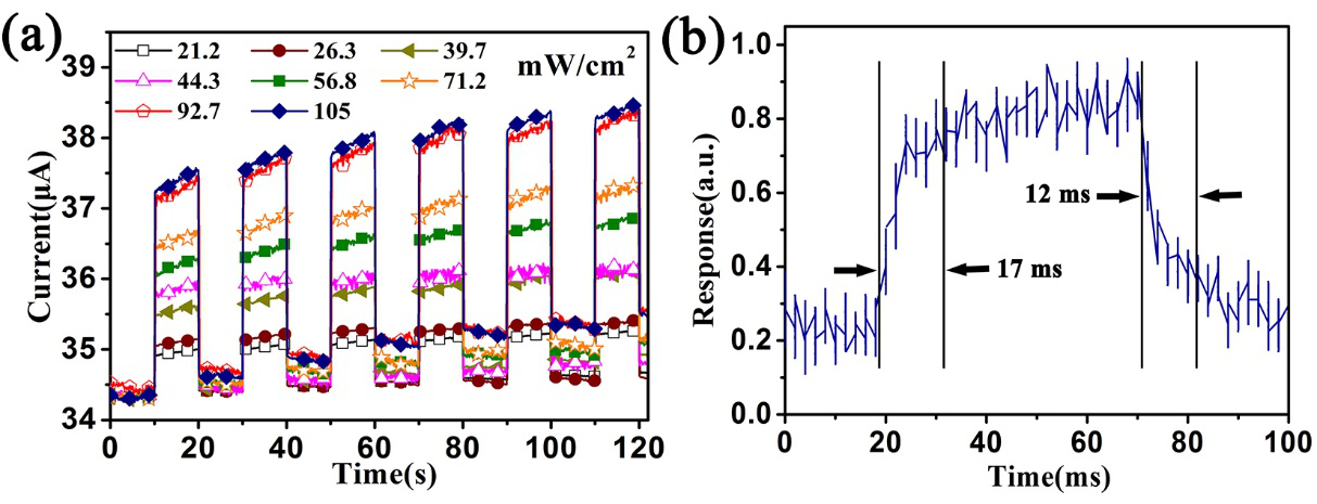
This device shows a good repeatable and stable response corresponding to the light illumination varying cyclically (Figure 2). As the incident light intensity is 105 mW/cm2 with the bias voltage of 3V, the device have the responsivity of 160.3 mA/W, a high detectivity of 6.5 × 10⁸ Jones, a fast rise and decay time of 17 and 12 ms.
These results pave the way for an effective approach to fabricate large scale ordered semiconductor nanowire arrays and promising photoelectric detectors.
This work was supported by National Basic Research Program of China (973 Program), the National Natural Science Foundation of China and the Foundation of Director of Institute of Solid State Physics, the Chinese Academy of Sciences.
Link to the paper: Preparation of large scale and highly ordered vanadium pentoxide (V2O5) nanowire arrays towards high performance photodetectors

Figure 1. (a) Digital photograph of ordered pine needles array structure, which was induced by rainwash. (b) SEM images of a highly ordered V2O5 nanowire array under different magnifications.(Image by FU Wenbiao)

Figure 2. (a) Photocurrent versus time curve of the photodetector device with the light intensity changing from 21.2 to 105mW/cm2 at a voltage of 3 V. (b) Rise and decay curves of the device measured by using a chopper with a frequency of 10 Hz. (Image by FU Wenbiao)
Dr. FEI Guangtao
Institute of Solid State Physics (http://english.issp.ac.cn/)
Tel: 86-551-65591453
Email: gtfei@issp.ac.cn
 Tel: +86-551-65591206
 Fax: +86-551-65591270
 Emai: zhous@hfcas.ac.cn
 350 Shushanhu Road