

Using first-principles calculations, Chinese researchers reported a giant TER effect of around 623%, which is comparable to 3D FTJs, can be realized through the ferroelectric tunnel junction constructed with the 2D ferroelectric materials BiP and B/N-doped graphene.
Ferroelectric tunnel junctions (FTJs) have attracted great interest for their potential applications in nonvolatile memories due to the tunnel electroresistance (TER) effect. So far, almost all FTJs studied focus on adopting three dimensional (3D) ferroelectric materials as the tunnel barrier and metal or semiconductor as the leads.
However, for thin films of 3D ferroelectric materials, the ferroelectricity will fade away when the thickness of the ferroelectric materials is decreased below a critical thickness because of the charge accumulation on their surfaces. Such a limit in the critical thickness of the ferroelectric layer is in contradiction with the technological demand of on-going device miniaturization.
Lately, many 2D ferroelectric materials with in-plane or out-of-plane spontaneous polarization have been theoretically presented such as monolayer Group IV chalcogenides, III2–VI3 van der Waals materials, elemental Group V monolayer materials with buckled structure and even 2D perovskite oxide thin films. Some of them, such as In2Se3, have been realized experimentally. Due to their atomic thickness, such materials should be good choices for overcoming the above critical thickness problem inherent in 3D FTJs.
However, up to now, very little is known about whether such 2D ferroelectric materials may lead to an excellent TER effect in FTJs.
In a recent study, ZHENG Xiaohong’s research group at Institute of Solid State Physics, Hefei Institutes of Physical Science adopted the 2D ferroelectric Group-V compound BiP, which is structurally analogous to phosphorene, as the central ferroelectric tunneling barrier and graphene/BiP vertical van der Waals (vdW) heterostructures as the left and right led to build an all 2D FTJ.
To differentiate the two leads, the graphene in the left and right leads was doped with B and N atoms, respectively. By density functional theory calculations, the scientists obtained a giant TER ratio of around 623%, which was comparable to 3D FTJs. The analysis of effective potential and electronic structure indicated that the large TER ratio arose from the unsymmetrical screening effects of the B/N-doped vertical van der Waals graphene/BiP leads. The findings demonstrated the great potential of novel application of 2D ferroelectric BiP in FTJs.
Link to the paper: Realizing giant tunneling electroresistance in two-dimensional graphene/BiP ferroelectric tunnel junction
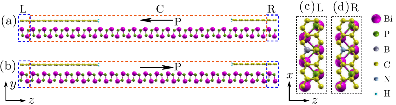
Schematic plot of the FTJ: (a) for polarization pointing to left and (b) for polarization pointing to right. The left/right leads are B/N-doped graphene/BiP vdW vertical heterostructures while the channel is the single layer 2D ferroelectric BiP. (c) and (d) are the top views of one supercell of the left (L) and right (R) leads shown in (a). (Image by KANG Lili)
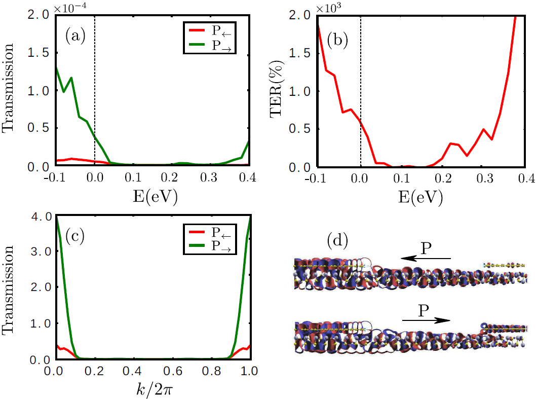
(a) The transmission function for both polarization directions; (b) the TER ratio as a function of electron energy; (c) the k-resolved contribution to the transmission at the Fermi level; (d) the scattering states incoming from the left lead at (E, k) = (0, 0) for both polarization directions. (Image by KANG Lili)
Contact:
ZHOU Shu
Hefei Institutes of Physical Science (http://english.hf.cas.cn/)
Email: zhous@hfcas.ac.cn
 Tel: +86-551-65591206
 Fax: +86-551-65591270
 Emai: zhous@hfcas.ac.cn
 350 Shushanhu Road