Organic semiconductor nanostructures (OSNs) usually exhibit unique optical and electrical properties superior to those of their bulk counterparts. Today, OSNs have been widely applied in modern optoelectronic devices, such as screens of mobile phone, sensors of acid gas, and photovoltaic.
Although the modulations of the morphologies, optical and electrical properties have great significance for the better application of OSNs, the morphology controlled growth of single crystalline samples still remains a challenge.
Dr. HAN Yuyan from High Magnetic Field Laboratory, Chinese Academy of Sciences (CHMFL) prepared high quality single crystalline nanostructures (NS) (e.g., particles, nanorods or nanowires) of perylene-3,4,9,10-tetracarboxylic dianhydride (PTCDA, a common organic semiconductor molecule) on porous anodic alumina oxide (AAO) substrate. It was found that the active sites with smaller curvature radius on AAO promote the nucleation of the NS. Consequently the NS morphologies can be simply modulated by controlling the substrate temperature.
The color of the main emission of PTCDA NS changes from orange to red (i.e., the wavelength varies from 610 nm to 700 nm). The AAO is nearly transparent to visible light and possesses excellent thermal and mechanical stabilities, which is helpful for the preparation of optoelectronic devices. It also should be mentioned that electrical conductivity of the single crystalline nanowire is much higher than that for the conventional polycrystalline film.
These results are very promising for the wider applications of functional organic semiconductors in modern optoelectronic devices.
Findings entitled “Preparation, Optical and Electrical Properties of PTCDA Nanostructures” were published in Nanoscale.
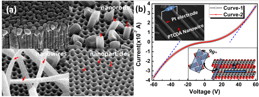
Figure 1. (a) SEM images of PTCDA film, nanorods, nanowires and nanoparticles, (b) the I-V curves of PTCDA nanowire measured by two-terminal technique, the up and down insets illustrate the measurement schematic and electron flow in PTCDA NW respectively.(Image by HAN Yuyan)