


Recently, a potent and selective enhancer of zeste homolog 2 (EZH2) inhibitor IHMT-EZH2-115 was discovered by a team led by Prof. LIU Qingsong from Hefei Institutes of Physical Science, Chinese Academy of Sciences, for the treatment of B-cell lymphomas.
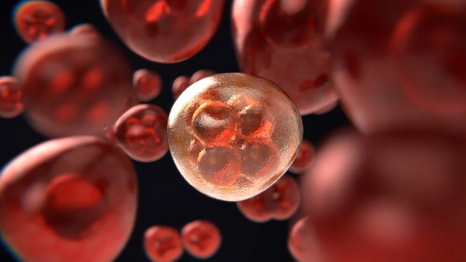
CMs (nonspherical clusters of a small number of particles) have potential applications in coatings, material self-assembly, biomedical diagnostics. The sphere has the smallest surface area under a certain volume, that is, the total Gibbs free energy of the surface is the lowest. Therefore, most nanoparticles exhibit spherical shape, leading to difficult preparation of non-spherical CMs.
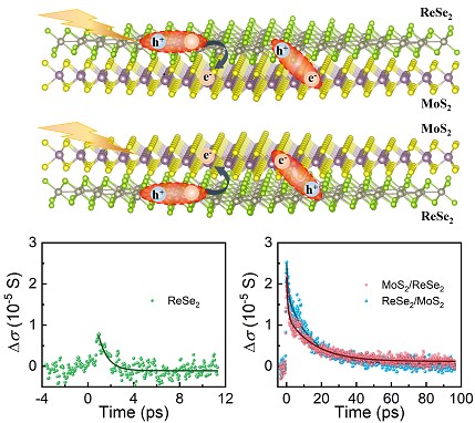
Recently, a collaborated team led by Professor SU Fuhai from Hefei Institutes of Physical Science (HFIPS), Chinese Academy of Sciences (CAS), successfully Identified the ultrafast dynamics in monolayer MoS2/ReSe2 heterostructures.

The Institute of Plasma Physics (ASIPP) researchers made a breakthrough in the subject of integrated Edge Localized Mode (ELM) and the divertor power flux control. "This time we take the lead in demonstrating the integrated ELM and divertor power flux control in target plasmas with parameters close to International Thermonuclear Experimental Reactor (ITER) high fusion gain (Q) operation using the Resonant Magnetic Perturbations (RMP),” said Prof. SUN Youwen from ASIPP, who led the team.
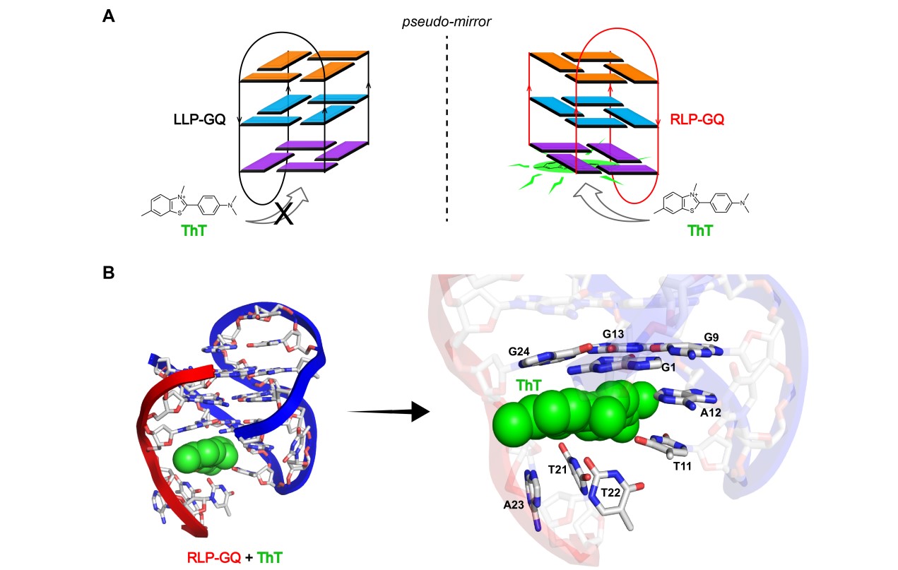
Human telomeric DNA consists of a tandem array of the G-rich repeat unit d(GGGTTA). A four-stranded helical structure adopted by G-rich sequences was named G-quadruplex (GQ) under physiological condition. The final 3'-terminal residue of the telomeric DNA G-overhang is inherently less precise.