

ZHENG Xiaohong’s research group at Institute of Solid State Physics, Hefei Institutes of Physical Science design a 2D out-of-plane ferroelectric tunnel junction adopting the graphene/In2Se3 van der Waals(vdW) vertical heterostructure as left/right lead and In2Se3 as the central ferroelectric tunneling barrier.
By density functional calculations combined with a nonequilibrium Green’s function technique, the scientists obtain a giant TER ratio of around 1 × 10⁸% in two-dimensional ferroelectric tunnel junctions with out-of-plane ferroelectric polarization, which is higher than that of most current 3D FTJs.
Ferroelectric tunnel junctions (FTJs), which use ferroelectric materials as the central tunnel barrier and metal or semiconductor as leads, have been widely studied due to their potential applications in nonvolatile memory devices.
It is well known that there is a limit in critical thickness of 3D ferroelectric materials for the observation of spontaneous polarization because of the charge accumulation on the surfaces, which is in contradiction with requirements in the device miniaturization.
To solve this problem, an emerging direction is the search of two-dimensional (2D) ferroelectric materials, which provides a natural good candidate for construction of devices with atomic thickness.
The team designed a 2D out-of-plane ferroelectric tunnel junction adopting the graphene/In2Se3 van der Waals(vdW) vertical heterostructure as left/right lead and In2Se3 as the central ferroelectric tunneling barrier.
By density functional calculations combined with a nonequilibrium Green’s function technique, the scientists obtained a giant TER ratio of around 1 × 10⁸%, which was higher than that of most current 3D FTJs.
Further analysis indicated that the big difference (~2.396 eV) in work functions of the two surfaces of the In2Se3 slab led to different charge transfer from graphene to In2Se3 and different electron filling of the bands of In2Se3 around the Fermi level when it contacted with graphene, which led to the change between the metallic and insulating nature of In2Se3.
Thus, an extremely high TER ratio could be easily achieved. The findings demonstrated the great potential of novel application of 2D ferroelectric material with out-of-plane ferroelectric polarization.
Link to the paper: Giant tunneling electroresistance in two-dimensional ferroelectric tunnel junctions with out-of-plane ferroelectric polarization
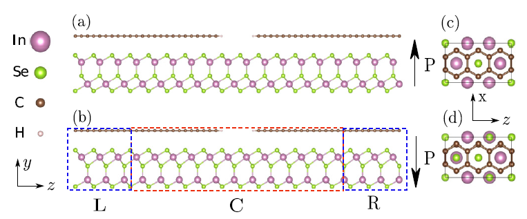
The structure of the FTJ with (a) upward polarization and (b) downward polarization. The structure is divided into three parts: left (L) and right (R) leads, and the central scattering region (C). The left/right leads are graphene/In2Se3 vdW vertical heterostructure. The channel is 2D In2Se3. Panels (c) and (d) are the top views of the lead for upward and downward polarizations, respectively. (Image by KANG Lili)
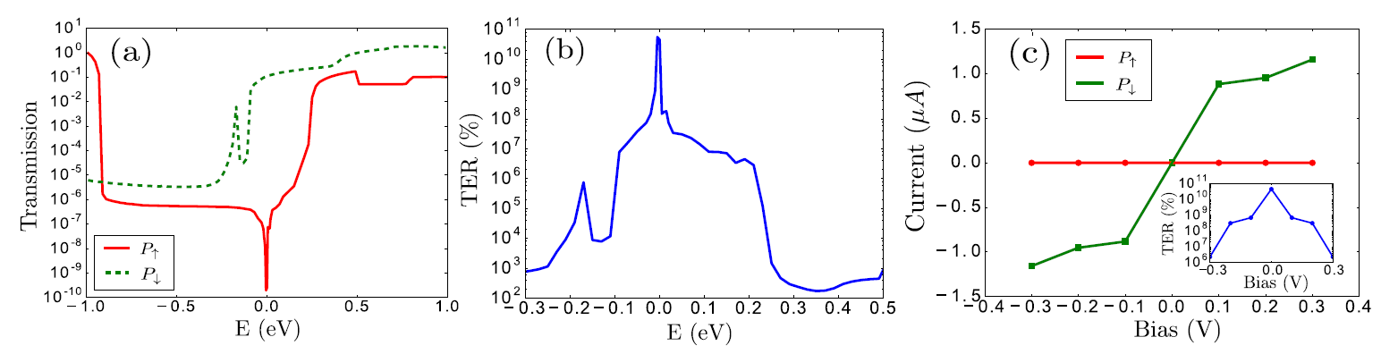
The transmission function for both polarization directions, with the Fermi level set to 0 eV; (b) the TER ratio as a function of electron energy; (c) the I-V curves for both polarization directions, with the inset showing the TER at low bias. (Image by KANG Lili)
Contact:
ZHOU Shu
Hefei Institutes of Physical Science (http://english.hf.cas.cn/)
Email: zhous@hfcas.ac.cn
 Tel: +86-551-65591206
 Fax: +86-551-65591270
 Emai: zhous@hfcas.ac.cn
 350 Shushanhu Road